
ICE40 Power Testing
Motivation
When designing a device such as the ICE40Ultra Plus FPGA into a system, its essential to know how it behaves under various conditions, especially when powerred by a battery.
This blog is to document experiments that show the actual power consumption under various conditions.
Setup
- The hardware used is the iCE40 breakout board from Lattice. This board was chosen as it breaks out all power rails of the FPGA.
- I used the PCF file from the UPduino as its identical. The absolutely wonderful icestorm toolchain was used as its very fast and scriptable. I would expect comparable results from the vendors Radiant toolchain.
- Current on each rail was measured using a Joulescope JS110.
- A toy math example is provided where two 8 bit counters are multiplied together to get a 16 bit result on every clock cycle.
Results
The data is located in the ice40_power Github page and not duplicated here.
Observations
- Done LED connection take 150uA! Disconnect this for lowest power.
- The RGB driver takes ~280uA, setting the CURREN or the RGBLEDEN to zero drops this current entirely.
- Holding the FPGA in reset or leaving it unconfigured consumes more power than if its programmed with an actual low power design.
- Enabling pullup resistors on inputs did not change the power consumption at all. This is likely due to the IO not picking up much interference. Touching the IO in this state causes power to go up.
- Mapping math to a DSP slice makes sense from the power point of view, in the above toy example, we save about 110uA.
- A minimally functional FPGA (10kHz, 24 bit counter) can consume as little as 4.4*1.219 + 3.76*3.3 + 3.4*3.3 + 1.5*3.3 + 96.3*1.219 = 151uW. The power consumption with such a low clock rate does not change significantly with increasing design size (a 1536 wide counter causes the core current to increase by 3uA). This implies that the FPGA will work quite well if used in a system where the clock can be dropped to 10kHz for long periods of time. The 10kHz clock allows the FPGA to respond to an interrupt and also switch to a faster clock. Alternatively, the clock can be completely halted on this FPGA as well if supplied by an external clock as shown by the halted clock test.
Bootup
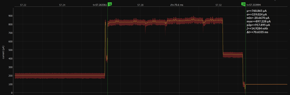
The FPGA boots from Flash programmed with low power 10kHz design. The FPGA configures itself from flash and draws power on the core and SPI flash bank (Bank 1) as shown below. The total energy consumption numbers as well as boot times are important for applications that will power off the FPGA and require it to boot up infrequently for power saving. As shown in the plots below, booting from the flash consumes about 46nAh of energy and takes about 70ms from start to finish. Note that this does not include the flash chip power consumption!


Future work
- Check out power when mapping to BRAM vs. registers
- Power consumption of IO banks with voltage and driving known loads
- Any other ideas?
