

A customer was using the UPduino v2.1 low-cost Lattice iCE40 FPGA board in their prototype to check out some IP in the FPGA. This IP required the use of a Phase Locked Loop (PLL) within the FPGA to generate specific frequencies that the design required.
The customer reported that the FPGA PLL was going out of lock intermittently.
Background
Phase locked loops are useful blocks (and there is one in the Lattice iCE40 UP5K FPGA) used to generate specific clock frequencies that may not necessarily be an integer multiple of a reference clock. The principle of operation is covered very well in this Wikipedia article.
The UPduino 2.1 is a low cost FPGA board thats designed for fast prototyping. The board has a couple of voltage regulators, an FT232H USB to SPI bridge, flash for FPGA code storage and supporting passives. The board is laid out on 2 layers.

Debug
Test Case
I was able to duplicate the failure mode on my setup which consisted of an UPduino connected to the customers test board. By a process of elimination, I was able to get the PLL to fail with an FPGA design consisting of the PLL, an output clock from the PLL, a GPIO input and an LED output from the FPGA. This rather minimal design exhibited the symptoms described by the user in a significantly more complex design.
On to Debug
Now that I had the test case, it was time to delve deeper: why would such a simple design cause the PLL to lose lock and that too by toggling a switch to the FPGA! This strange behavior was also not consistent: pushing the switch would intermittently cause the PLL to go out of lock. There didn't appear to be any pattern to the behavior either.
I was also able to eliminate the customer board as the source of the issue. I checked all DC power supplies on the UPduino and customer board with a multi-meter, things looked good. Searching online gave me a hint on what to pursue next, (isn't information sharing a wonderful thing!) ie. clock quality and board layout.
From my experience, I knew that PLL's were finicky analog creatures and had to be cared for by low jitter input clocks and proper filtering of the power supply.
A simple change I made was to source a clean 12MHz clock from an external crystal instead of using the on-board resonator which has poor phase noise in comparison. This seemed to reduce the probability of PLL unlocking but didnt make the issue go away.

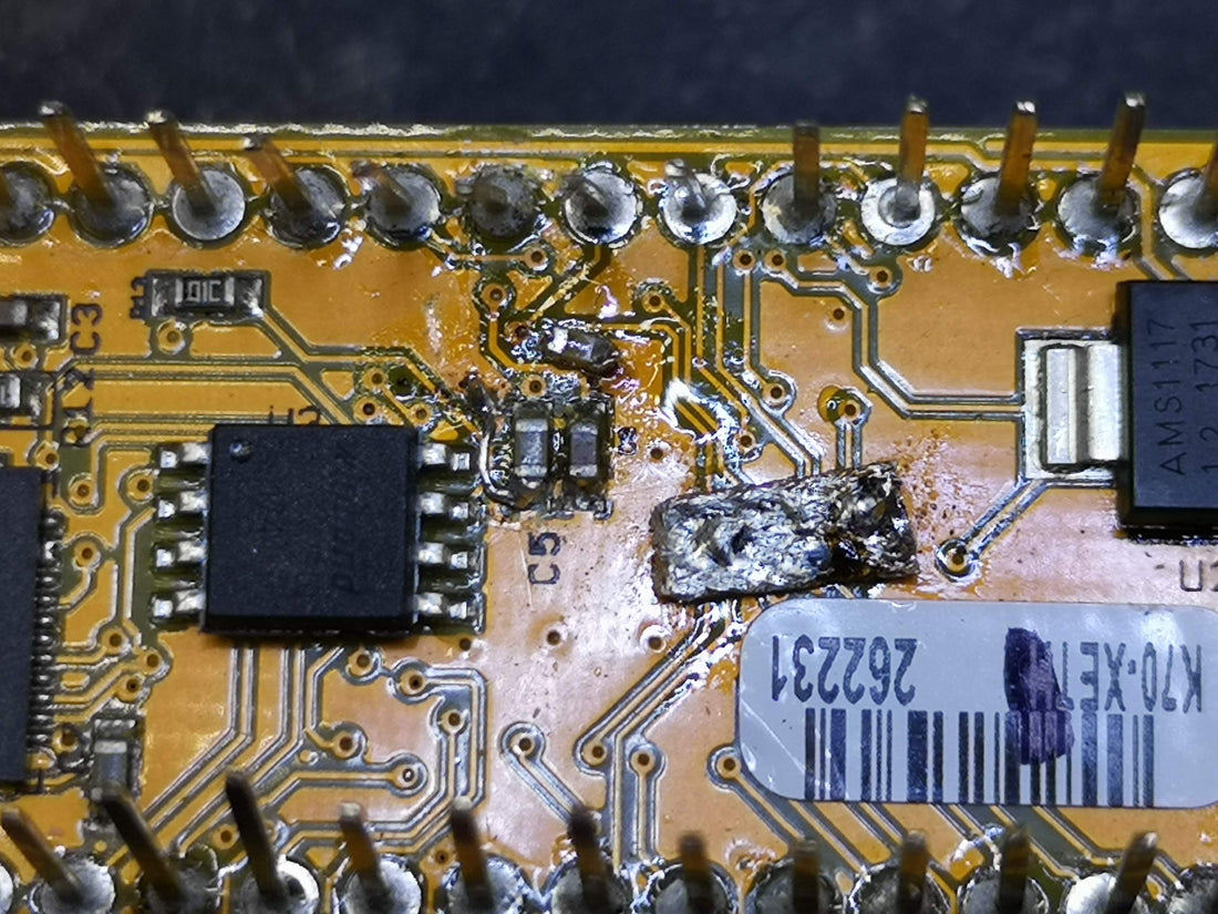
Power and Ground
The dedicated power supply on the PLL and the ground near it looked good with about 10-15mV of digital noise, not too bad. Its important to follow proper probing guidelines when making such measurements!
I probed the DC voltages and noticed a substantial noise of >50mV or so on the supplies. This was significantly reduced by adding 10uF caps on the LDO's. However, this didnt seem to improve the probability of the PLL losing lock.

I then measured the ground plane from one end of the board to the other. I was shocked to see huge spikes on the ground plane! This meant that the various circuits on the board had a different view of what they considered a reference.

The UPduino is a small board, about 2.2cm x 5.1cm. Having the ground plane be different by hundreds of mV across such a small board, that too with such a simple design on the FPGA, not consuming much power seemed to indicate something was very wrong!
I analyzed the board layout in Eagle and noticed that the Ground plane was routed on the bottom side as follows:

The solid filled areas are the ground plane in the above picture. As you can see, the ground plane is split into multiple discrete sections, never a good idea! This gave me a good idea of what to try next. I used copper braid to short across various sections of the ground plane and was able to get the noise down significantly. More importantly, this correlated well with a decreasing probability of the PLL failing to lock. A good indication that I was on the right track.

Unfortunately, all the hacking was not able to restore a reliable PLL lock on this board. Needless to say, the customer was unable to use this board for their design as the board design was to blame.
Next Steps and a New Beginning!
I had inherited the design from the original manufacturer/designer. This experience, as well as the feedback from users about various features missing from the UPduino, got me thinking about coming up with the next generation of the board.
UPduino 3.0!
I kicked off the next generation: the UPduino 3.0, with a goal of not just fixing the layout but adding significant features as documented on this GitHub site.
The ground plane on the UPduino 3.0 is a solid plane with no cuts. This was a hard requirement on the layout. The power plane does have some cuts but shouldn't be too significant as shown in the plots below. A detailed review was done to ensure that power and grounds had sufficiently thick traces and decoupling caps were placed close to the pins being decoupled. A 0.1uF/4.7uF capacitor combination was settled on as a standard decoupling strategy. Going to a 4 layer board made the design implementable: it was clear during routing of this board that the original design with 2 layers was simply not feasible and a bad design choice in the first place. The extra cost of going to 4 layers vs. 2 layers was simply not worth the risk.
The first version of the design is now complete and will be fabricated soon with a high expectation that the PLL will lock!
If you would like to be involved, please feel free to browse Discourse and/or join the Discord channel!